
Tools for controlling physics at the nanoscale are crucial for the development of new paradigms in optics, electronics and spintronics. We develop advanced techniques based on thermal scanning probe lithography (t-SPL) and direct laser writing, for crafting the physical properties of materials via physical, structural or chemical modifications.
We develop and use thermally assisted magnetic nanopatterning and laser lithography, in combination with nanolithography, for patterning multidimensional spin-textures in magnetic multilayers, such as domains, domain walls and topological solitons. Then, we use such spin textures for controlling and study the emission and propagation of spin waves in magnetic thin films. We study the three-dimensional propagation of spin waves in multilayers
We control at the nanoscale the electronic and spin transport properties of thin-films in phase-change materials and complex oxides, and develop new artificial nanomaterials and devices with engineered electronic transport properties, arising from the proximity and coexistence of different structural and electronic phases.
Advanced Nanofabrication and Phase Nanoengineering
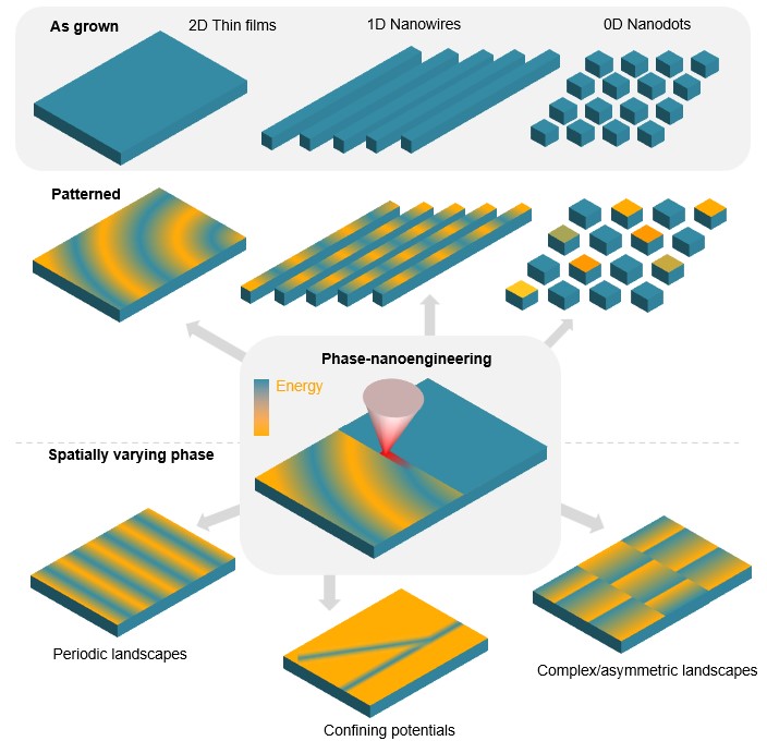
Nanomaterials acquire novel physical properties which derive from their specific nanostructure, or reduced dimensionality, and which can be markedly different from the properties of their bulk counterpart. Phase-nanoengineering (Figure 1) is based on directly inducing highly localized, tunable and stable modifications to the physical properties of materials via exposure with a highly localized energy source.
We use a highly localized energy source to irradiate point-by-point the material and induce controlled phase transitions, compositional or structural modifications. By tuning the energy source while scanning the sample, we control point-by-point the degree of modification, creating “grayscale” profiles which in turn lead to highly controlled physical properties. This goes beyond the capabilities of most conventional nanofabrication methodologies, which in most cases allow for binary patterns characterized by the presence or absence of the material.
The direct-writing process also has the advantage of not requiring to place the sample in contact with harsh chemicals, and of leaving completely untouched the non-patterned regions. This aspect is critical when dealing with sensitive materials, or in general materials which are not compatible with standard lithographic processes.
Depending on the geometry and properties of the energy landscape, with respect to the typical physical length-scales in play, widely different effects can be achieved. Periodic energy landscapes, such as the 1-D modulation shown in figure, can give rise to “grayscale” metamaterials such as magnonic or photonic crystals. Highly localized potentials on the other hand provide the basic building blocks for realizing nanoelectronic circuitry, e.g. nanowires, nano-islands, gates. Similarly, in the case of waves, sharp property modulations, such as the refractive index in optics or the magnetic properties in magnonics allow confining effects, among which waveguiding, or tailored wave emission.
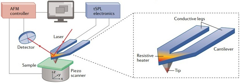
We develop and use Phase nanoengineering is performed via either Thermal Scanning Probe Lithography (tSPL, Figure 2) and Direct Laser Writing (DLW). In the first case, a nanometric heated Atomic Force Microscope tip is scanned over the sample surface, locally heating the surface controllably and sequentially. Its advantages are the sub-10 nm spatial resolution, high degree of tunability of the tip temperature,
from room temperature up to about 1200°C , and flexibility for a wide range of materials and applications. DLW on the other hand provides higher peak powers compared to tSPL, and diffraction-limited spatial resolution. By combining and developing the two techniques, a wide range of systems ranging from magnetic materials, to 2D and quantum materials can be investigated.
Selected references
E. Albisetti, A. Calò, A. Zanut, X. Zheng, G.M. de Peppo, and E. Riedo, “Thermal scanning probe lithography”, Nature Reviews Methods Primers 2, 32 (2022).
E. Albisetti, D. Petti, R. Bertacco, E. Riedo, “Magnetic nanopatterning via thermal scanning probe lithography”, Book chapter in “Nanofabrication”, Edited by José Maria De Teresa, IOP Publishing (2020).
E. Albisetti, D. Petti, M. Pancaldi, M. Madami, S. Tacchi, J. Curtis, W. P. King, A. Papp, G. Csaba, W. Porod, P. Vavassori, E. Riedo, R. Bertacco, “Nanopatterning reconfigurable magnetic landscapes via thermally assisted scanning probe lithography”, Nature Nanotechnology, 11 (6), 545–551 (2016).
X. Zheng, A. Calò, E. Albisetti, X. Liu, A. S. M. Alharbi, G. Arefe, X. Liu, M. Spieser, W. J. Yoo, T. Taniguchi, K. Watanabe, C. Aruta, A. Ciarrocchi, A. Kis, B.S. Lee, M. Lipson, J. Hone, D. Shahrjerdi, E. Riedo, “Direct metal contacts on MoS2 with vanishing Schottky barrier via thermal nanolithography”, Nature Electronics, 2, 17–25 (2019).
X. Zheng, A. Calò, T. Cao, X. Liu, Z. Huang, P. M. Das, M. Drndic, E. Albisetti, F. Lavin, T. Li, V. Narang, W. P. King, J. W. Harrold, M. Vittadello, C. Aruta, D. Shahrjerdi, E. Riedo, “Spatial defects nanoengineering for bipolar conductivity in MoS2”, Nature Communications, 11, 1–12 (2020).
Nanomagnetism and Magnonics
Spin textures in magnetic materials, such as magnetic domains, domain walls or skyrmions, are extremely interesing for their potential as active components in data storage and processing devices. The interest arises from their scalability towards nanoscale dimensions, resilience against external perturbations and high degree of tunability via external stimuli. For example, racetrack memories are based on storing and manipulating information in domain walls or skyrmions, which are controllably stabilized and manipulated in ferromagnetic nanowires. Also, the dynamic properties of spin textures, i.e. their excitations, and the way they interact with spin waves, i.e. propagating magnetic excitations, are a very active field of reasearch for both fundamental science and applications in technology. With the rising of spin textures, and the discovery of complex textures in ferromagnets and antiferromagnets alike, the importance of controlling their properties and configuration has become crucial.
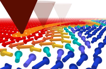
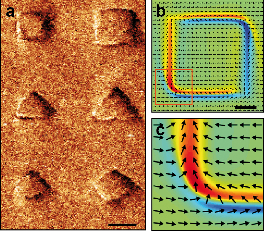
Recently, we introduced a novel technique, thermally assisted magnetic scanning probe lithography (tam-SPL), to write nanoscale reconfigurable spin-textures in a continuous and homogeneous film. In tam-SPL, we use the heatable tip of a scanning probe microscope, in presence of a magnetic field, to heat the portion of the film in contact to the tip and then we exploit the cooling due to heat dispersion when the tip is moved to another position. This confined “field cooling” causes a local pinning of the magnetization of the FM along the direction of the applied magnetic field, which reflects in a shift of its hysteresis loop. This method allows writing of arbitrary shaped spin-textures such as magnetic domains, domain walls or solitons, with controlled magnetic anisotropy and spin-orientation (Figure 3 a-c). The patterned spin textures can be modulated via external fields but, importantly, are stable at remanence and cannot be permanently erased with magnetic fields.
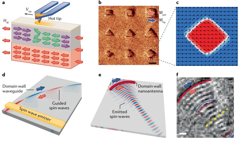
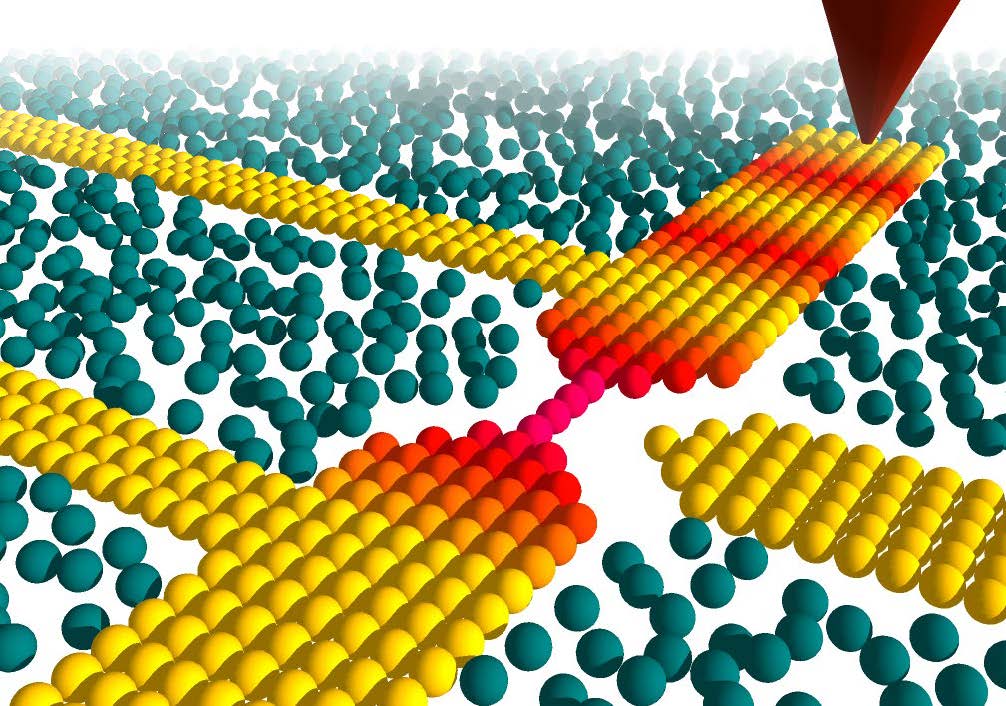
The precise control of the magnetization allows for various applications. Among these, manipulating spin waves using patterned spin textures is an extremely promising strategy. Indeed, spin waves are being extensively studied as a potential platform for beyond-CMOS computing, owing to their rich phenomenology, energy efficiency and nanoscale dimensions. In figure 3 d-f we show two applications in this field. In (d), tam-SPL spin textures are used as waveguides for confining and steering spin waves on-chip, and for building the basic building blocks for reconfigurable circuits.
In (e-f), on the other hand, domain walls in a synthetic antiferromagnt are used as magnonic nanoantennas for emitting shaped spin-wave wavefronts. Further applications are envisioned; for example, patterning of out-of-plane magnetized materials and 3D spin textures, and the realization of magnon-based computing platforms that exploit spin-wave interference in continuous films.
Selected references
D. Petti, S. Tacchi, and E. Albisetti, “Review on magnonics with engineered spin textures”, Journal of Physics D: Applied Physics, 55, 293003 (2022).
A. Barman, G. Gubbiotti, S. Ladak, A. O. Adeyeye, M. Krawczyk, J. Gräfe, C. Adelmann, Sorin Cotofana, A. Naeemi, V. I Vasyuchka, B.Hillebrands, SA Nikitov, H. Yu, D. Grundler, A. Sadovnikov, A.A. Grachev, S.E. Sheshukova, J.-Y. Duquesne, M. Marangolo, G. Csaba, W. Porod, V.E. Demidov, S. Urazhdin, S. Demokritov, E. Albisetti, D. Petti, R. Bertacco, H. Schulteiss et al., “The 2021 Magnonics Roadmap”, Journal of Physics: Condensed Matter, 33, 413001 (2021).
E. Albisetti, S. Tacchi, R. Silvani, G. Scaramuzzi, S. Finizio, S. Wintz, C. Rinaldi, M. Cantoni, J. Raabe, G. Carlotti, R. Bertacco, E. Riedo, D. Petti, “Optically Inspired Nanomagnonics with Nonreciprocal Spin Waves in Synthetic Antiferromagnets,” Advanced Materials, 32, 1906439 (2020).
E. Albisetti, D. Petti, G. Sala, R. Silvani, S. Tacchi, S. Finizio, S. Wintz, A. Caló, X. Zheng, J. Raabe, E. Riedo, R. Bertacco “Nanoscale spin-wave circuits based on engineered reconfigurable spin-textures,” Communications Physics, 1, 56 (2018).
E. Albisetti, D. Petti, R. Bertacco, E. Riedo, “Magnetic nanopatterning via thermal scanning probe lithography”, Book chapter in “Nanofabrication”, Edited by José Maria De Teresa, IOP Publishing (2020).
Nanoelectronics & Quantum Materials
Work in progress..