
Our activities involve a range of techniques for the growth of thin films and heterostructures, the nanoscale and bulk characterization, the nanofabrication and simulations.
Advanced Nanofabrication
Thermal Scanning Probe Lithography (tSPL) + Laser Writing – NanoFrazor Explore
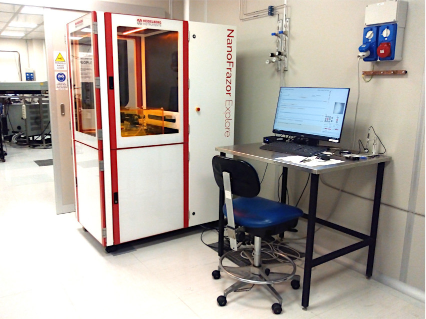
The Heidelberg NanoFrazor Explore is a dedicated Thermal Scanning Probe Lithography nanofabrication tool. It uses a ultra-sharp heatable probe tip for locally heating the substrate with sub-10 resolution. It is also equipped with a laser writer module for allowing mix-and-match tSPL and laser lithography. It allows in-situ imaging, markerless alignment, 3D nanopatterning capabilities with < 1 nm vertical resolution. The NanoFrazor equipped with a tuable magnetic field is used for performing thermally assisted magnetic scanning probe lithography (tam-SPL).
Thermal Scanning Probe Lithography (tSPL) – Keysight 5600LS
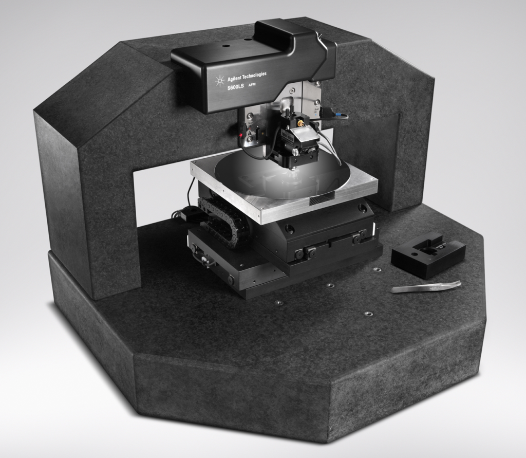
tSPL and tamSPL are performed also using a customized 5600LS AFM system. The 5600LS AFM allows imaging of both large samples (in air) and small samples (in air, or in liquid under temperature control). The 5600LS utilizes a 200 mm x 200 mm, fully addressable and programmable stage, as well as a low-noise AFM design. Samples up to 8” in diameter and 30mm tall are easily accepted by the 200mm vacuum chuck. The stage accommodates a 300 mm wafer with repositioning.
Optical / E-beam lithography – PoliFab

Micro-nanofabrication techniques such as equipment for performing Optical / EBeam lithography are available in PoliFab, the micro-nanofabrication center of Politecnico di Milano
Characterization
Scanning Probe Microscopy – Park NX 10
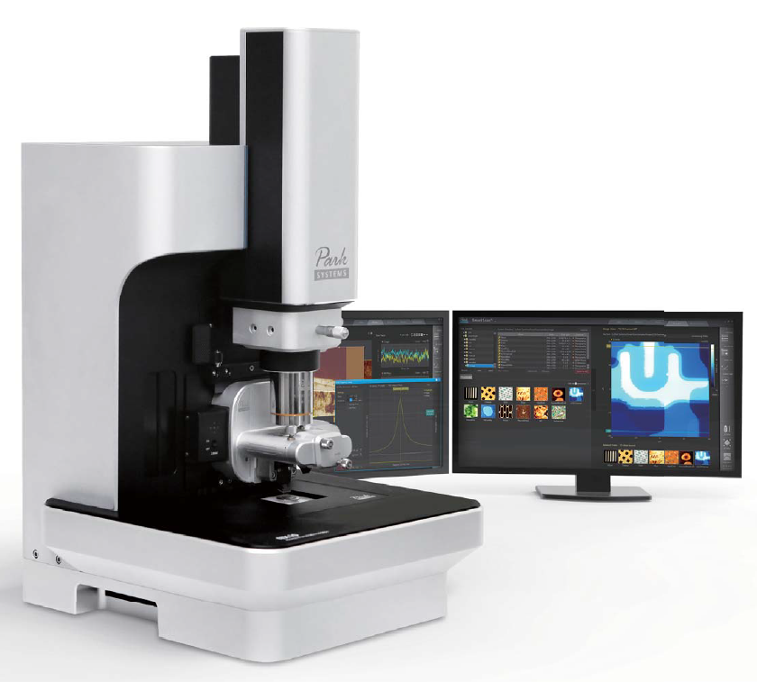
The Park NX 10 Scanning Probe Microscope allows to characterize with nanoscale resolution the morphology, electrical / magnetic properties, nanomechanical and thermal properties of a wide range of systems. A motorized coarse positioning system allows to investigate samples up to 2×2 cm2. The microscope is equipped with an 100×100 um2 in-plane piezoscanner. Measurements mode available include: AFM, Magnetic Force Microscopy in a variable magnetic field, Conductive-AFM, Kelvin Probe Force Microscopy, Piezo-Force Microscopy, Scanning Thermal Microscopy, Nanomechanics. A heatable stage from RT up to 250°C can be employed.
Kerr Magnetometry and Kerr Microscopy
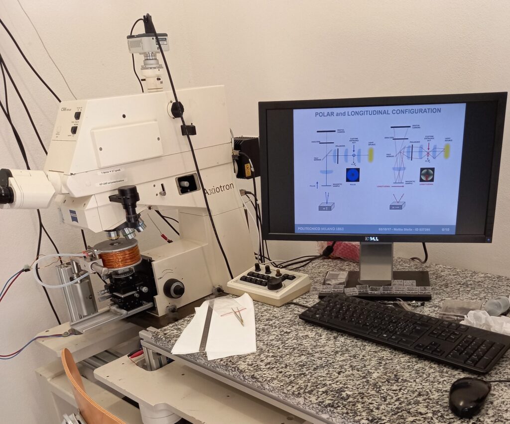
The Magneto-Optical Kerr Effect (MOKE) provides a powerful way for studying the magnetic behaviour of thin films by simply analyzing the light reflected from their surface. The incident light is polarized linearly before reaching the sample; the reflected light is analyzed through a polarizer (the analyzer). Two different setups are used depending on the application:
- The table-top MOKE setup uses laser light from a 532 nm diode, focused on the sample surface. The longitudinal or polar configuration give access to the in-plane or out-of-plane component of the magnetization with respect to the sample surface, as a function of the external magnetic field.
- The MOKE Microscope allows to acquire images with magnetic contrast, as a function of the external magnetic field. It uses Kohler illumination via a high intensity LED lamp.
Vibrating Sample Magnetometry (VSM)
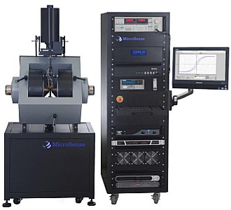
The Microsense, LLC. Easy VSM model EZ-9A allows to measure quantitatively the magnetic properties of the samples. A maximum field of 2.25 T can be applied, and it can measure magnetic moments down to μemu. It allows a fully automated rotation of the sample of 360° and it is possible to support operations with a temperature ranging from 100 K to 1000 K and a temperature rate up to 60-100 K/min.
Electronic transport measurements
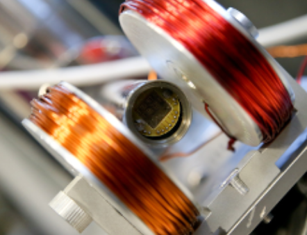
Transport measurements are performed either via probes or wire bonding using different setups. Measurements include I-V curves, magnetoresistance, Hall effect.
- Table top 4-point or 2-point probe measurements for room temperature measurements as a function of the external magnetic field.
- Electrical measurements in the temperature range 10 K-450 K are performed using a closed circuit He cryostat (Displex CS-202NE from ARS).
Growth of thin films
Magnetron Sputtering – AJA ATC Orion 8
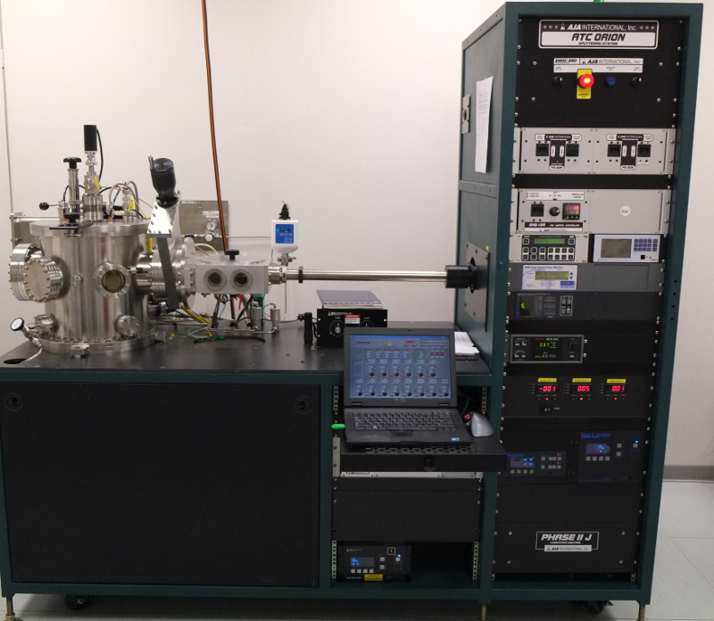
Equipment for deposition of thin films using magnetron sputtering on 3” substrates. Typical use: growth of magnetic heterostructures and dielectric materials deposition. The AJA system is provided with ten 2”/1”, DC and/or RF, magnetron sputtering sources, which are arranged in a confocal, sputtering-up configuration. The system allows to deposit multilayer structures with precise and automatic control of film thickness.
Modelling and Simulations
Workstation
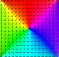
A dedicated Workstation equipped with a GeForce RTX 3080 Ti GPU, an Intel Core i9-12900K CPU and 128 GB RAM is used for performing finite element simulations and other labor-intensive tasks. Examples are MuMax3/OOMMF for performing micromagnetic simulations or COMSOL.